Flip-chip Packages And Chipped Acceptance Criteria
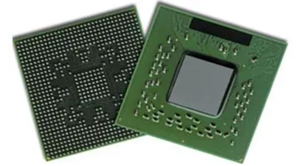
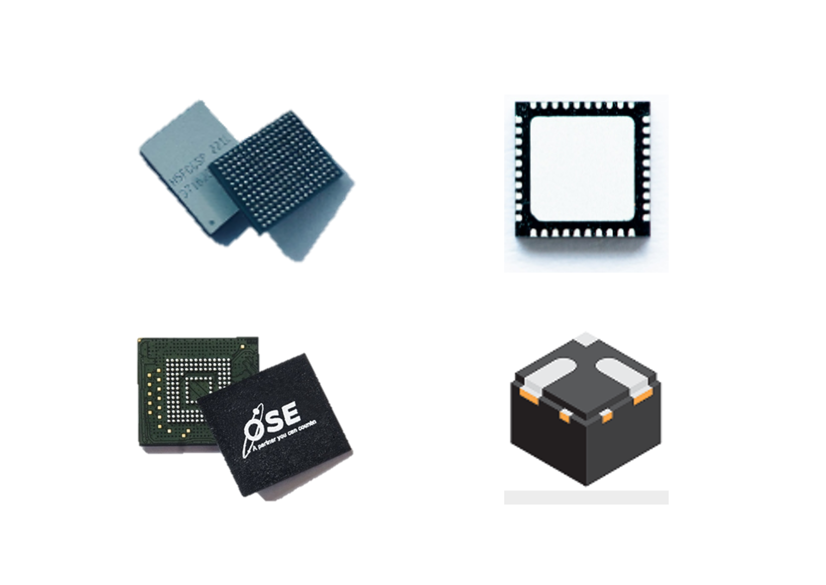
Imagine peering into a microscopic world, a landscape of shimmering gold bumps and intricate silicon pathways. Here, tiny chips, the brains of our devices, are flipped and precisely nestled onto their packages, a critical step in creating the technology that powers our lives. This is the realm of flip-chip packaging, a technology experiencing both incredible advancements and a fascinating debate about acceptance criteria.
At the heart of this story lies a fundamental question: How do we define "good enough" when dealing with components at the nanometer scale? The rise of flip-chip technology has brought unparalleled performance, but also a new set of challenges in inspection and quality control. This article explores the evolving landscape of flip-chip packaging and the "chipped acceptance criteria" that are shaping its future, examining the significance of these criteria for the industry and the implications for the reliability and performance of our electronic devices.
The Rise of Flip-Chip: A Technological Leap
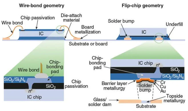
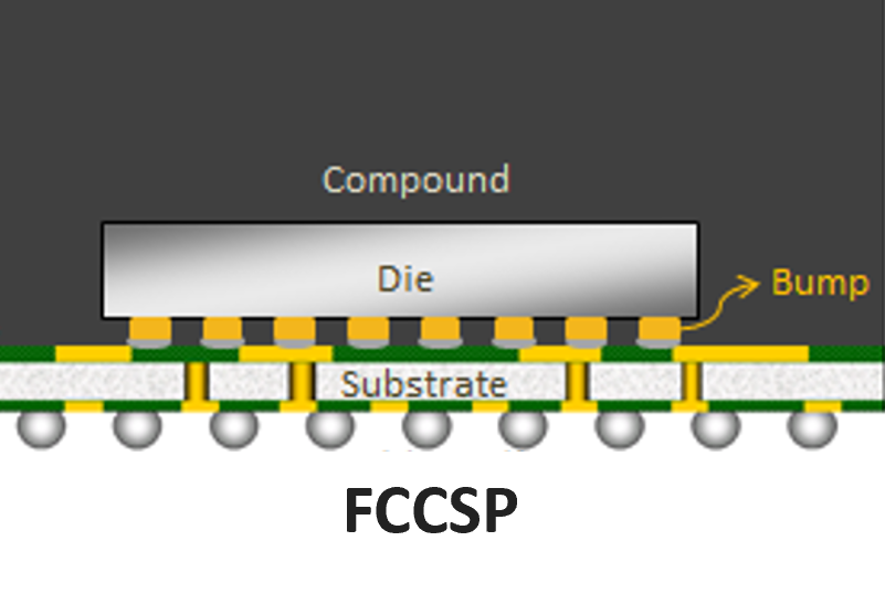
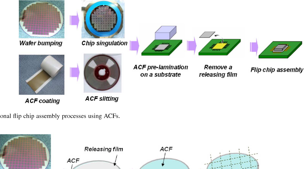
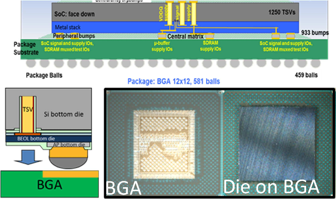
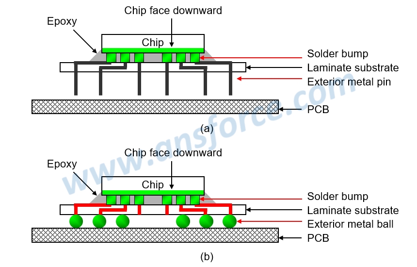
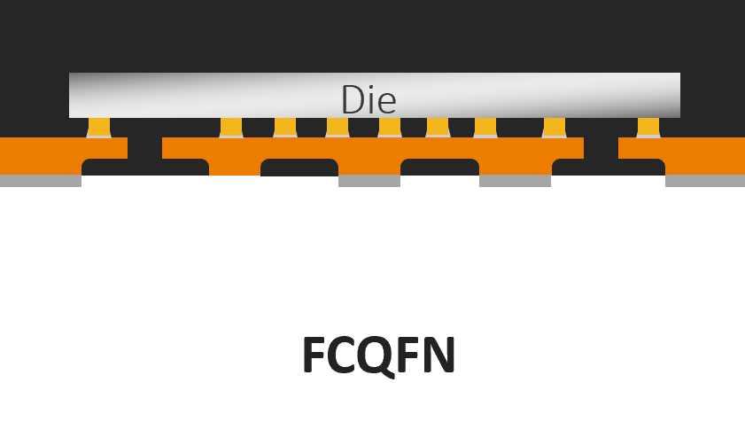
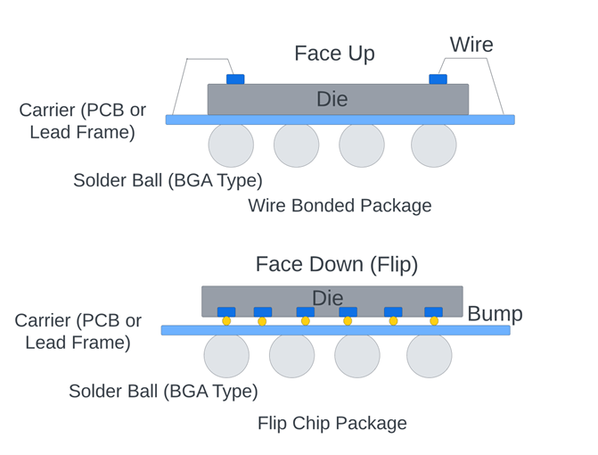
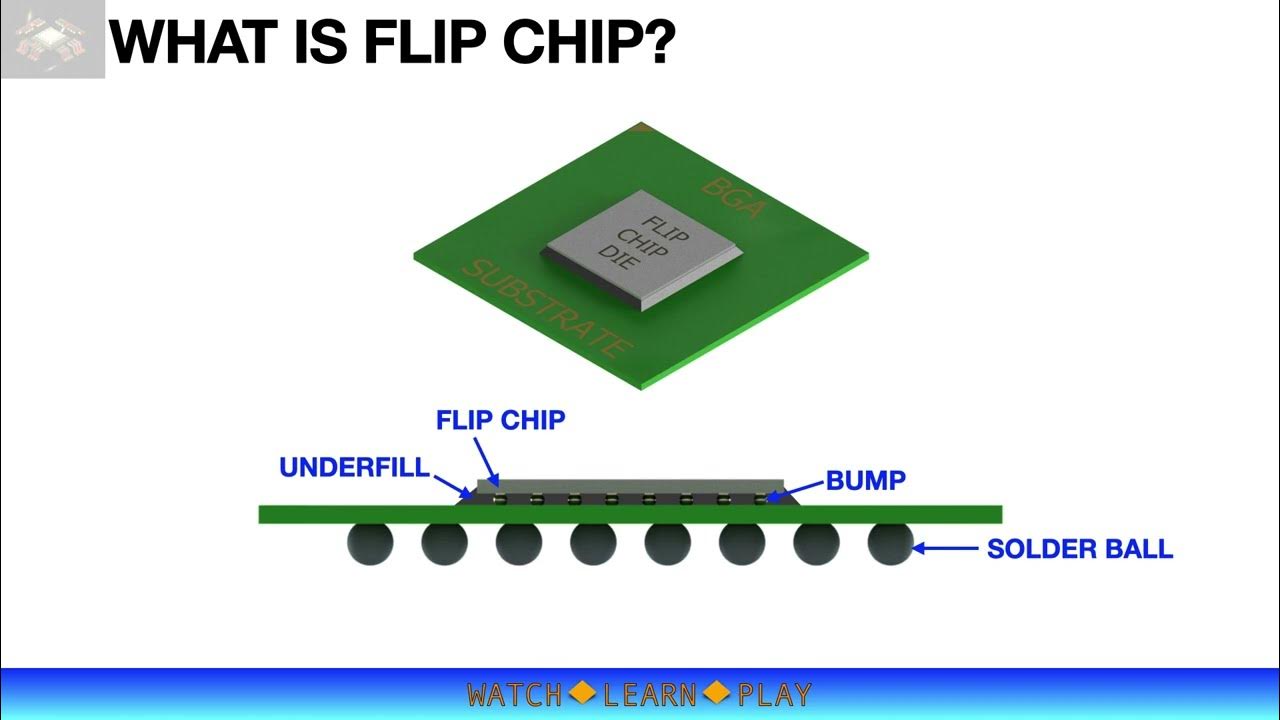
Traditional wire bonding, where tiny wires connect the chip to the package, has long been the standard. However, as chips become smaller and faster, wire bonding's limitations become apparent. Flip-chip technology overcomes these limitations by directly attaching the chip face-down onto the package substrate.
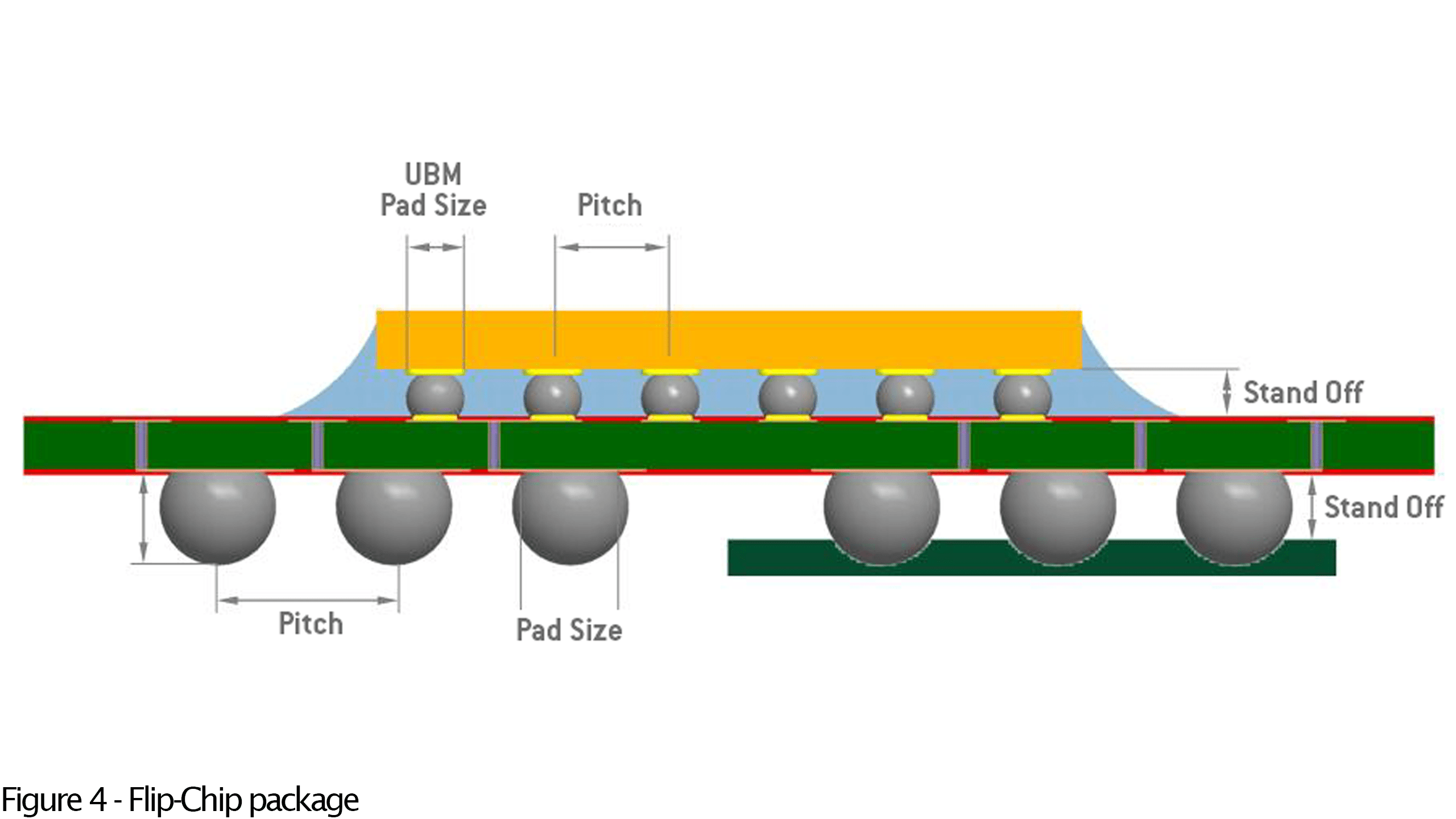
This direct connection, often achieved using solder bumps or copper pillars, offers several advantages. These advantages include shorter signal paths, improved electrical performance, and enhanced thermal dissipation, all crucial for today's high-performance electronics.
According to a report by Mordor Intelligence, the flip-chip market is expected to continue its strong growth trajectory. This growth is driven by the increasing demand for smaller, faster, and more power-efficient devices in areas like mobile computing, automotive, and high-performance computing.
The Imperfection Paradox: Defining "Good Enough"
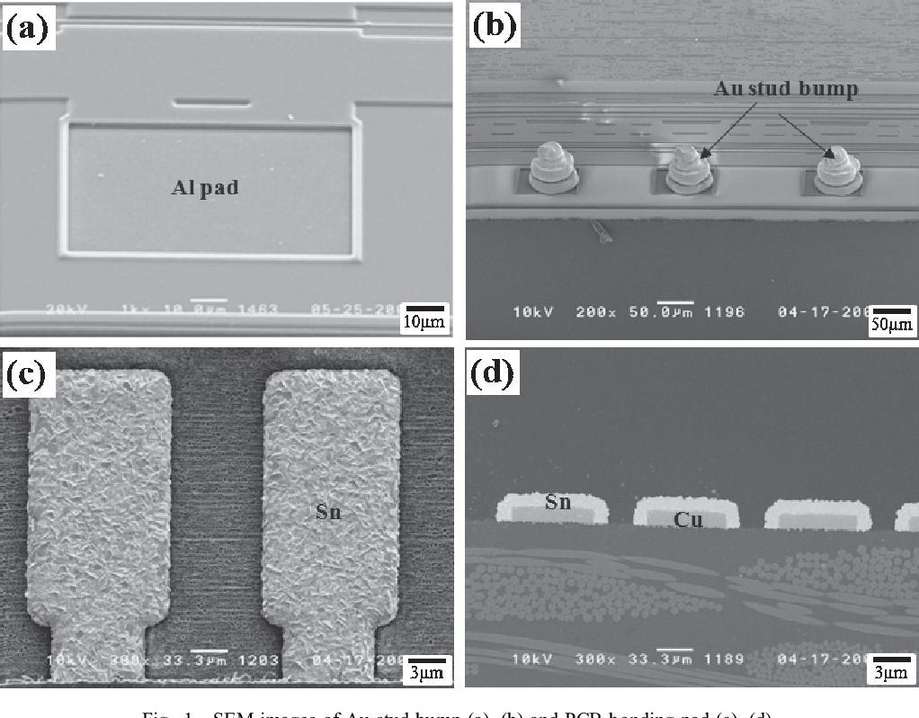
The increased density and complexity of flip-chip interconnections present significant inspection challenges. Visual inspection, X-ray analysis, and other techniques are used to identify defects such as voids in the solder bumps, misalignment, or cracks.
The challenge lies in defining what level of imperfection is acceptable. This is where the debate around "chipped acceptance criteria" comes into play. Are we striving for perfection, which is often costly and potentially unachievable, or can we tolerate a certain level of imperfection without compromising reliability and performance?
Dr. Emily Carter, a leading expert in microelectronics packaging at the Institute of Electrical and Electronics Engineers (IEEE), explains, "The key is to understand the impact of these imperfections on the long-term reliability of the device. Not all defects are created equal; some may be benign, while others can lead to premature failure."
Understanding Different Types of Defects
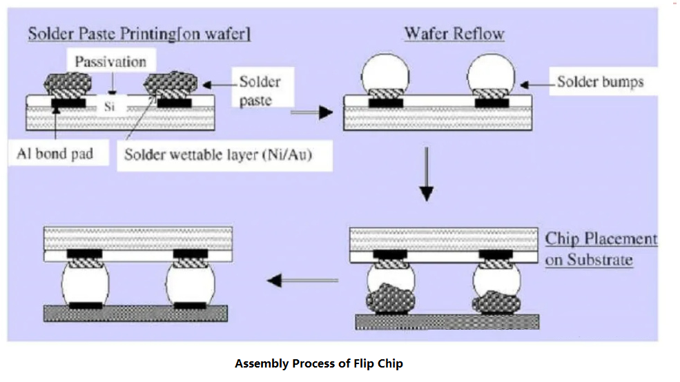
Several types of defects can occur during flip-chip assembly. Solder voids, small air pockets within the solder joints, are a common occurrence. Minor misalignment of the chip on the package is another frequent issue. Cracks in the solder or the underfill material (a protective epoxy) can also arise.
Each of these defects has a different potential impact on the device's reliability. Large voids, for example, can weaken the solder joint and lead to fatigue failure under thermal cycling. Similarly, significant misalignment can stress the interconnections and reduce their lifespan.
Therefore, acceptance criteria need to be tailored to the specific application and the criticality of the device. For instance, a high-reliability application, such as aerospace electronics, will demand stricter acceptance criteria than a consumer electronics application where a lower failure rate is acceptable.
The Role of Simulation and Modeling
Advanced simulation and modeling techniques are playing an increasingly important role in determining acceptable defect levels. These techniques allow engineers to predict the impact of different defects on the mechanical, thermal, and electrical performance of the flip-chip assembly.
By simulating the device's behavior under various operating conditions, it is possible to identify the defects that are most likely to lead to failure. This information can then be used to establish realistic and effective acceptance criteria.
For example, Finite Element Analysis (FEA) is a powerful tool for simulating the stress and strain distribution within the solder joints under thermal cycling. This can help to determine the maximum allowable void size or misalignment that can be tolerated without compromising reliability. The Semiconductor Industry Association (SIA) is actively promoting the use of these advanced techniques.
The Economic Considerations
The stringency of acceptance criteria also has significant economic implications. Striving for perfection can significantly increase manufacturing costs, as more intensive inspection and rework are required.
Moreover, overly strict acceptance criteria can lead to the rejection of perfectly functional devices, further increasing costs and reducing yield. Therefore, it is essential to strike a balance between quality and cost when defining acceptance criteria.
Companies are increasingly adopting a risk-based approach to acceptance criteria, where the level of inspection and the allowable defect levels are determined based on the potential consequences of failure. This approach helps to optimize the trade-off between quality and cost.
Looking Ahead: The Future of Flip-Chip Acceptance
The future of flip-chip packaging is likely to see even greater integration of simulation and modeling into the acceptance process. As chips become more complex and feature sizes shrink, traditional inspection techniques will become increasingly challenging.
Advanced non-destructive testing methods, such as acoustic microscopy and terahertz imaging, are also being developed to improve defect detection capabilities. These techniques offer the potential to detect defects that are not visible using traditional methods.
Furthermore, the industry is moving towards a more data-driven approach to quality control. By collecting and analyzing data from the manufacturing process, it is possible to identify the root causes of defects and implement process improvements to reduce their occurrence.
John Thompson, a senior analyst at TechSearch International, a leading market research firm, predicts that "the adoption of artificial intelligence (AI) and machine learning (ML) will play a significant role in future inspection systems. AI-powered systems can learn to identify subtle defects and predict potential failures with greater accuracy than traditional methods."
Embracing Imperfection, Ensuring Reliability
The story of flip-chip packaging and acceptance criteria is a reminder that even in the pursuit of technological perfection, a degree of imperfection is often unavoidable, and even acceptable. The key is to understand the limits of that imperfection and to develop robust methods for ensuring reliability.
By embracing advanced simulation techniques, adopting a risk-based approach, and leveraging the power of data analytics, the industry can continue to push the boundaries of flip-chip technology while maintaining the high levels of quality and reliability that are essential for the future of electronics.
Ultimately, the evolution of "chipped acceptance criteria" reflects a growing maturity in the understanding and management of complex microelectronic systems. It's a journey of constant learning, adaptation, and innovation, ensuring that the tiny brains within our devices continue to function reliably and efficiently, powering the world around us.