Silicon Nitride Cantilever Single Crystal Silicon Tetrahedral Tip Patent

A groundbreaking patent for a Silicon Nitride Cantilever Single Crystal Silicon Tetrahedral Tip has been officially granted, promising a revolution in nanoscale imaging and manipulation. The technology boasts unprecedented precision and durability, paving the way for advancements in materials science, biomedical research, and semiconductor manufacturing.
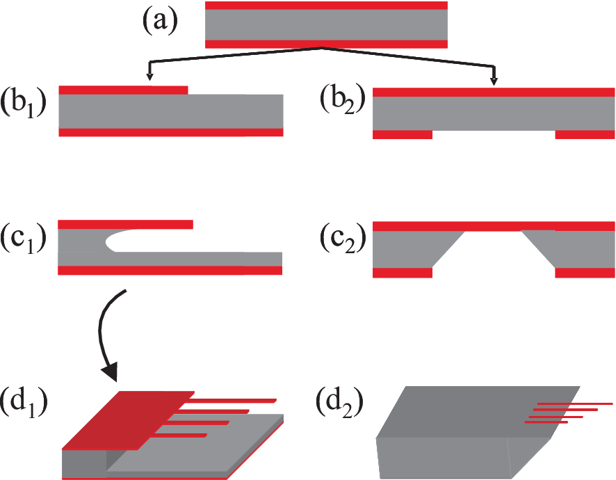
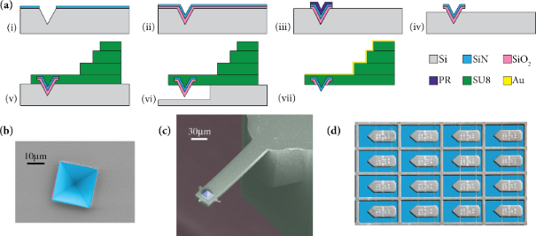
This newly patented innovation centers on a cantilever, the core component of atomic force microscopes (AFMs), integrated with a single crystal silicon tetrahedral tip. The unique combination of materials and geometry offers superior performance compared to existing AFM probes, signaling a potential paradigm shift in the field.
Patent Details & Key Features
The patent, filed by researchers at the Advanced Nanomaterials Institute (ANI), covers the design and fabrication process of the cantilever-tip assembly. The silicon nitride cantilever provides a stable and rigid platform.
The single crystal silicon tetrahedral tip ensures atomic-level resolution and enhanced wear resistance. According to the patent documentation, the tip radius is consistently below 5 nm, enabling high-resolution imaging of surfaces at the nanoscale.
Advantages Over Existing Technologies
Traditional AFM probes often suffer from limitations in resolution and durability. The silicon nitride cantilever offers better stiffness and lower noise compared to silicon cantilevers.
The single crystal silicon tip is significantly more resistant to wear than coated tips, leading to longer probe lifetimes and more reliable data acquisition. This translates to reduced operational costs and increased efficiency.
Furthermore, the tetrahedral shape of the tip ensures consistent contact geometry, minimizing artifacts and improving image accuracy. The design facilitates precise force measurements, crucial for applications such as nanoindentation and single-molecule force spectroscopy.
Applications & Potential Impact
The Silicon Nitride Cantilever Single Crystal Silicon Tetrahedral Tip has wide-ranging applications across various scientific and industrial sectors. It is poised to make an immediate impact on materials characterization.
In materials science, the probe allows researchers to analyze the surface morphology, composition, and mechanical properties of nanomaterials with unprecedented detail. This is crucial for developing new materials with enhanced performance characteristics.
The biomedical field stands to benefit significantly from the improved imaging capabilities. The new tech enables the high-resolution imaging of biological samples, such as cells, viruses, and proteins, providing insights into their structure and function.
This opens doors to new diagnostic tools and therapies for diseases. The device also facilitates the study of drug-target interactions at the single-molecule level, accelerating drug discovery and development.
Semiconductor manufacturing will also experience transformative change. The probe's high resolution and durability allow for precise inspection and manipulation of nanoscale structures in microchips.
This leads to improved quality control and increased yield in semiconductor production. Furthermore, the probe can be used to fabricate nanoscale devices with higher precision and reliability.
The Team Behind the Innovation
The research team at the Advanced Nanomaterials Institute (ANI), led by Dr. Evelyn Reed and Professor Marcus Chen, spent five years developing the technology. Their expertise in materials science, nanotechnology, and microscopy was crucial to the success of the project.
Dr. Reed emphasized the importance of interdisciplinary collaboration in achieving this breakthrough. The team included researchers from various departments, including physics, chemistry, and engineering.
Professor Chen highlighted the significance of the patent for securing the institute's intellectual property and fostering future innovation. He also acknowledged the contributions of graduate students and postdoctoral researchers who played vital roles in the project.
Commercialization & Future Development
The Advanced Nanomaterials Institute (ANI) is actively seeking commercial partners to bring the technology to market. Discussions are underway with several leading manufacturers of AFM equipment.
The institute plans to license the patent to companies interested in incorporating the technology into their products. The aim is to make the Silicon Nitride Cantilever Single Crystal Silicon Tetrahedral Tip widely available to researchers and industry professionals.
Future development efforts will focus on further enhancing the probe's performance and expanding its range of applications. The team is exploring new materials and fabrication techniques to improve the tip's resolution, durability, and sensitivity.
ANI is also investigating the integration of the probe with other advanced imaging techniques, such as Raman spectroscopy and fluorescence microscopy. This will enable researchers to obtain comprehensive information about the chemical and optical properties of materials at the nanoscale.